Exploring Hardware Problems (With Verilog)
24 min. read
I want to explore a few different hardware design problems that I have encountered in various different settings in the past 6-12 months, be it at university or elsewhere. In studying this material, I have noticed that there are, increasingly, very few good quality resources that document this topic to any satisfying depth, so the hope here is that I can at least add a small positive vector that direction. I’ll present a few sample problems here, and let’s be clear from the outset that these are not optimal solutions in any capacity. Perhaps one of the alluring things about these problems is that, barring seasoned expertise, finding an optimal solution is not generally a straightforward or procedural matter.
What is Hardware Design?
This is a particular subdomain of electrical engineering and computer systems that is becoming evermore present with the prevalence of (micro)processors, IoT devices and many other chip-based technologies in our everyday lives. Being currently in the midst of completing a Bachelor degree of Computer Science, I can well attest to the fact that in this discipline, as well as in software engineering, we tend to treat the vehicle of our livelihoods - computers - as black boxes, not especially concerned with the implementation details, just the fact it can compute what we want it to compute. Even having done some units learning how to solve algorithmic problems with assembly languages like MIPS, coursework of this kind skims over how those instructions are actually carried out within the computer architecture itself.
Hardware design, then, is interested in the low-level components flip-flops and multiplexors that underpin the functioning of such devices. Whilst falling out of prevalence for some time, in recent years this subject as seen a marked resurgence, with many companies turning towards low-latency compute devices like FPGAs to support their software infrastructure. One such example are algorithmic trading companies like Jane Street, Optiver and IMC, where squeezing the most out of every nanosecond of clock time is worth many dollars, with many zeros after it.
So, here I want consider some interview-style problems that I saw when applying for such a company, in the hopes that we might explore how to think about hardware design and why it should garner such attention in the first place.
Hardware vs. Software
Before jumping in, I want to make explicit why we would even be interested in hardware design. Aren’t computers getting super, super fast! Yes, but also no. That is, your computer or phone does so many different things - processing graphics, running the OS kernel, etc., not to mention any of the programs or pieces of software you are wanting to run on top of that, that the gains in computing power we see don’t necessarily make software like computers the absolute fastest for raw computation. If raw computation is all you care about, then you don’t need a screen, speakers, and so forth. You also don’t need a kernel. You just want to run your algorithm on bare hardware. This is where hardware design is so useful. Because despite most FPGAs having clocks slower than any personal computer, by stripping all the extra frills from it, it turns out to be non-trivially faster when it comes to computation.
Problem One: Pattern Matching
Suppose we are receiving a data stream from some server, and want to design an on-line (that is, it receives the input serially) hardware unit that will receive this input and assert a particular output bit high when a specified pattern is observed.
| Signal Name | Direction | Width (bits) | Description/behaviour |
|---|---|---|---|
clk | Input | 1 | Clock module |
reset | Input | 1 | Active high reset |
in_valid | Input | 1 | High when incoming data byte is valid, else 0 |
in_stream | Input | 8 | ASCII character (only either ‘A’ or ‘B’) |
pattern_match | Output | 1 | High when the specified pattern is received |
Aside: ASCII
A brief tangent on ASCII values:
we humans like to communicate with letters, computers less so. They only
understand bits (1’s and 0’s), so when I type on a keyboard, a keystroke
like the letter ‘A’ needs to be encoded into a bit pattern, transmitted
from the peripheral device, then decoded at the display. ASCII is one
such encoding schema and it uses 8 bits, meaning there are
280x41 which in binary is 01000001. This will be important in a
second.
Back to the question at hand. Let’s go through each signal to make sure we are on the same page here:
clk- every computing device has what’s called a Clock which is a module used to synchronise the behaviour of the entire device. A standard sort of Intel computer might have a 5.00 GHz clock, which means it oscillates 5 × 109= 5, 000, 000, 000 times a second. Each oscillation corresponds to the execution of a particular instruction so in theory your computer accomplishes 5 billion things a second! However, each of these instructions are very basic - it might be writing a value to memory, reading a value to memory, or adding two values together. Each keystroke might correspond to many clock oscillations. If you then think about all the background tasks your computer runs without you knowing, and the number of such simple instructions you’d have to run to render, say, a video, 5 billion doesn’t quite seem like so much. Anyway, low-level devices like an FPGA also have a clock and the goal is to use as few of these clock cycles as we can to achieve the desired behaviour. No wastage if possible! reset- imagine this as an override switch. When it is activated, the system will go back to its starting configuration and all prior work will be lost. Note that it is <Highlight text=”active high” />, as compared to active low. Active high means that it is logic 1 when activated.in_valid- when this is asserted high, we should actually do something with the data byte that we receive for that clock cycle. If not, we ignore it.in_stream- each clock cycle, we will receive a fresh byte (8 bits) of data corresponding to a particular character. Over many clock cycles, this will form the pattern we should match to.
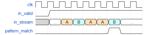
Example Output
Let’s say that the pattern we want to match is ‘ABAAB’. Then below is the desired timing behaviour we wish to produce:
Initial Solution
Before we worry about premature optimisation, we should always start
by crafting a basic working solution. The first thing to consider is the
type of problem we are dealing with. In hardware design, there are
generally two classes: sequential and combinatorial. In sequential
problems, the output depends on both the present **as well as** past
inputs. In combinatorial problems, the output depends only on the state
of the system at **that particular clock**. In our case, since we
receive each byte of the pattern one-by-one, once pattern_match has
read in some characters, it has to think back to earlier inputs it
received and recall whether they were the right ones. Clearly, then, we
have a sequential problem. Sequential problems require us to implement
some form of memory device. For more complicated, larger-scale problems,
you might opt for a RAM module, but for our purposes, something
straightforward like a flip-flop should do.
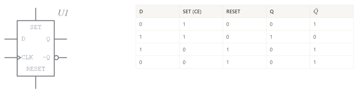
Specifically, a D flip-flop. First, its logic table:
And also its associated timing diagram1:
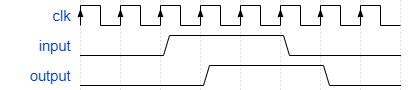
The actual gate-level implementation of a D flip-flop doesn’t concern us here, the key idea is this. represents the input to the flip-flop. When the (I will also use CE or clock-enable) is 1, then at the end of that clock cycle, the value on the line will appear at the output . just represents the negation of . When is high, no matter the value of , the output goes to 0. This is a 1 bit flip-flop - it can either store a 1 or a 0, however for our purposes we will abstract away the technical details and consider an 8 bit flip-flop where and are 8 bit bus lines.
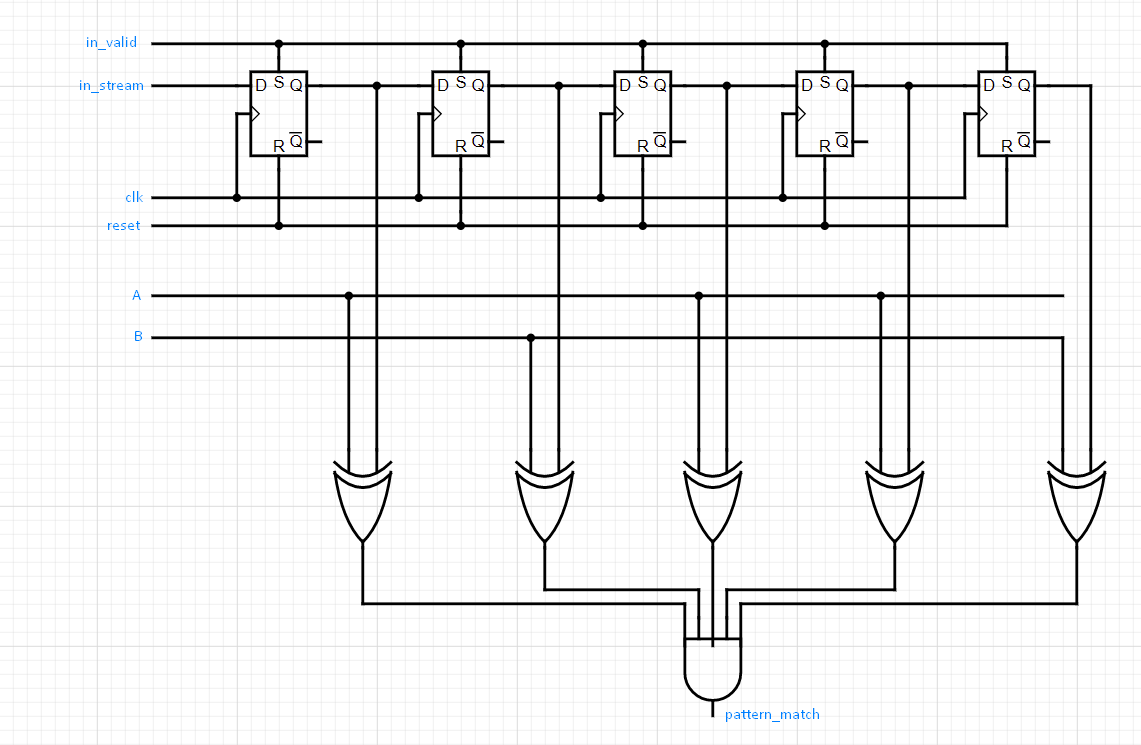
How is this helpful? Well, what we want to do is collect five bytes from the input data, somehow keep them all in front of us, then once the fifth one comes in perform some logic to decide whether we have a matching pattern or not. If we don’t then keep reading in data. If we do, then we need to output high. So what we could do, is connect five of these flip-flops in series so that the output of one goes into the input of another. After five clocks of reading valid data, we will have the last five bytes of data at hand that we can read and determine whether it matches or not.
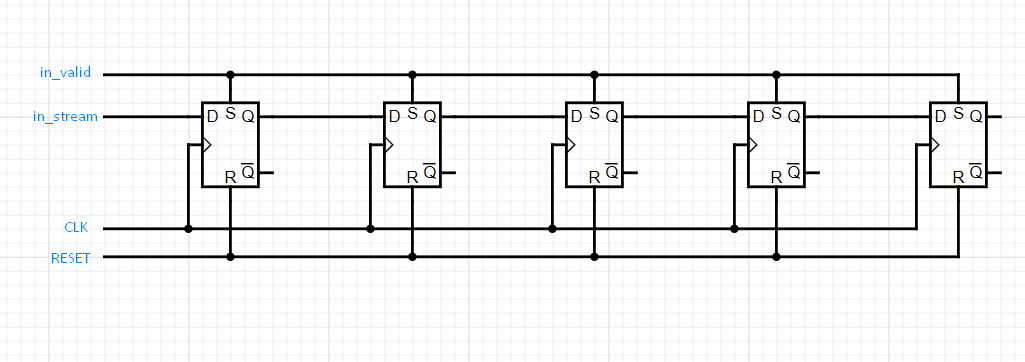
We connect the in_valid wire to the CE of the flip-flop, so that we
only adjust the flip-flop stored value when the next incoming byte
should be observed. We connect the CLK to synchronise the latching
action of the flip-flops, and the reset wire to the RESET of the
flip-flop. With this set-up, if we were reading in a stream such as
(from right to left), the values stored in our collective flip-flops
would be…:
And so on. Let’s now think about how to determine whether a given collection of characters in our memory unit constitutes a pattern match. Again, to abstract away the details, we will assume that the we have two 8-bit registers storing the encodings of ‘A’ and ‘B’. If we are matching ‘ABAAB’, then what we want is the 8 bits stored in the left-most flip-flop to match an ‘A’, the 8 bits in the next flip-flop to match a ‘B’ and so on. Think about a logic gate/device you may know of that compares the equality of two inputs. Hopefully you came up with an (⊕) gate2. Assuming we have access to an 8-bit gate, if we rip the value from each flip-flop output into this XOR gate along with either an ‘A’ or a ‘B’, then AND the result from all of these, we will have our desired output. Each XOR gate checks that a given flip-flop matched its part of the sequence, then the AND gate checks that all flip-flops matched their part of the sequence.
Optimising The Solution
But wait! It turns out that this solution doesn’t satisfy the timing constraints. We are actually wasting a clock cycle somewhere, can you spot where? And remember, one clock cycle might be fractions of a second, but at scale this accumulates into a lot of ineffective compute time. Additionally, by using fewer physical components, the footprint of our design improves too!
It turns out that we only need four, rather than five, flip-flops.
Because once that fifth value comes in, we want to decide on that same
clock cycle whether the pattern matches or not. Currently, the fifth
value is first loaded into the flip-flop, and only on the next cycle is
it passed into our comparator logic. This mean that if a pattern is
found, the high assertion on pattern_match will appear a clock cycle
later than we want it. So instead of utilising fifth flip-flop, we
simply pass the in_stream directly into one check of our comparator.
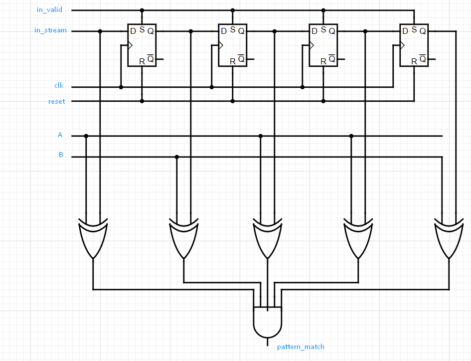
Ah, much better!
Alterations To The Problem
With these sorts of problems, we always want to give some thought to how this problem would scale if we broaden the constraints. Notice that in this solution, there were a few assumptions made:
- The
in_stream(and hence the pattern to match) could only contain ’A’s or ’B’s - The pattern to match was at most five characters long
What happens when we alter these conditions? Well, in the case of (1), it would mean that we would need to allocate more memory to storing the “magic” bit patterns corresponding to any of the characters that could appear in our pattern. Is this a big concern? Not really. Each address in the register is storing 8 bits, ^^so even if we had a massive collection of characters to match, say ≈ 1000 , then we would only be looking at around 1 kB of space, which is tiny. Typical RAM modules like the one we would need are, in their smallest form, on the scale of megabytes (1000’s of kB)^^. How about (2)? This problem gets considerably harder if the pattern you need to match has an arbitrary length or is specified at run-time. If it were fixed, but allowed to take an arbitrarily large value, then one may consider moving away from flip-flops, only because there are more efficient forms of memory storage that we could consider.
Problem Two: Verilog Synthesis
What is Verilog?
It’s all well and good to be able to, as we did above, consider a problem description and implement a solution directly into hardware, but there are two key issues we run into: 1) such solutions are brittle, because changing input parameters of the problem slightly more or less upends the original solution, and 2) this process doesn’t scale well for more advanced problems. Guaranteeing optimal computational complexity for anything at an industry-level of size would be no small feat indeed. Humans don’t think very well in terms of 1’s and 0’s, but we are pretty good at mapping problems into some sort of procedural algorithm. So why don’t we “design” our hardware in software and then let the computer transpile this into actual hardware. What a great idea…this is precisely what languages like Verilog and VHDL do. I might do a Verilog tutorial at a later date, but for now I’ll assume some familiarity with it. One important skill a hardware engineer needs to have is understanding how to write efficient Verilog code, and ^^furthermore understanding how their code will be synthesised at a hardware level^^. Inefficient synthesis is bad news!
The Problem Description
Suppose I gave you the following Verilog snippet:
1module looping(a, b, out)2 input [3:0] a, b;3 output out;45 always @ (a, b)6 begin7 out = 1b'0;8 for (int i = 0; i < 4; i++)9 begin10 if (a[i] == b[i])11 begin12 out <= a[i];13 break;14 end15 end16 end17endmodule18
I now ask you to describe how the Verilog transpiler would communicate this logic in hardware. Your response?
Solution
This algorithm looks innocent enough, but it’s worthwhile pondering what
is actually going on here. You have two four bit inputs a, b, each of
which you loop over bit-by-bit, working from least to most significant
(right to left). If any of the bits a and b match, you set out to
be this matching bit.
Okay. With something like this, instead of worrying about the inputs as
four bits, we need really only figure out what’s going on for one bit,
then extrapolate that out to the full input. It might help to consider a
truth table here for the output out at a particular loop:
a[i] | b[i] | out |
|---|---|---|
| 0 | 0 | a |
| 0 | 1 | 0 |
| 1 | 0 | 0 |
| 1 | 1 | a |
The key observation to make here, is that we are feeding one of two
possible outputs through to out depending on the particular
combination of a and b. Either we pass through a or we pass
through 0. Whenever you observe this sort of paradigm of selecting
one of a set of inputs as your final output, you should in general think
about a multiplexor (MUX). So for this particular truth table, we
might construct the following 2-to-1 MUX3:
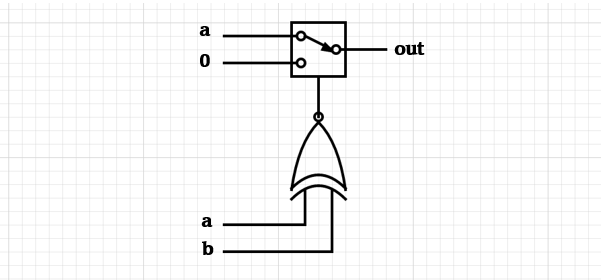
If we map a to the 0 line of the MUX, and a ground or 0 input to
the 1 line of the MUX, then our select line should be an XNOR gate,
which returns 0 when
, else 1. With one bit out of the way, it stands to reason that the
entire loop will synthesise to a set of concurrent MUXs. But in what
order? There are two observations to make here. The first is that we are
working from least to most significant bits, or right to left. The
second is that as soon as we hit a matching bit between a and b,
we break from the loop and set out as required. This means that the
least significant bit should form the final rung of the ladder, and the
most significant bit the initial rung. More precisely, the output of the
loop for bit N should feed into one of the input lines from the MUX
for bit N-1:
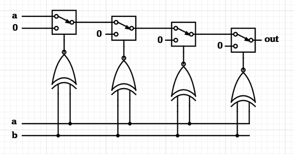
And there you have it! We were able to decode Verilog into its
constituent hardware. You could verify the correctness of this
implementation by writing a test bench for the Verilog module with
something like
Icarus4,
but for now I hope you can reason to yourself that this implementation
is in fact correct. It’s also worth considering how the synthesis would
alter if we change the action for a[i] == b[i].
- Note that we assume here a flip flop that samples the output on
the rising clock edge (indicated by the arrows), hence why there is
a full period of
inputbeing high before it is read by the flip-flop.↩ - A ⊕ B outputs 1 when A = B , else 0↩
- Ignore the fact that the MUX appears to be selecting
aas theout. This is just how the components are drawn with tools like circuit.diagram.org. In general either line could be selected by the MUX.↩ - Which I will hopefully cover in a tutorial in future…↩